

As the semiconductor industry pushes deeper into the nanoscale era, one challenge is becoming increasingly critical, seeing what lies beneath the surface of advanced chips. Modern semiconductor devices are now built using highly complex three dimensional architectures with layers and structures that are often too small and too deeply embedded for conventional inspection systems to measure accurately. For manufacturers producing the chips that power artificial intelligence, high performance computing, and advanced electronics, even minor measurement errors can lead to lower yields, higher costs, and production delays. Semiconductor metrology startup Invisix is developing a new approach designed to solve this growing visibility problem.
The company has raised an oversubscribed €20 million seed funding round backed by investors including Hitachi Ventures, Transition Ventures, imec.xpand, Doosan Investment, and a leading semiconductor manufacturer.
The new capital will support product development, team expansion, and customer engagement as the company moves toward commercial deployment of its first system.
Tackling a Growing Semiconductor Bottleneck
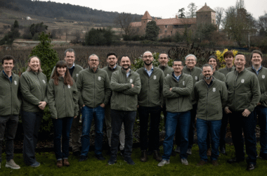
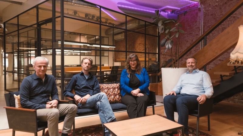
Founded by former ASML researchers and physicists Christina Porter and Sietse van der Post, Invisix is focused on advanced semiconductor metrology.
Metrology systems play a crucial role in chip manufacturing by measuring structures throughout the production process and ensuring each layer is correctly fabricated before additional layers are added.
As chip designs become smaller and more complex, conventional optical inspection tools are increasingly unable to accurately measure many of the buried nanoscale structures that determine overall device performance.
This challenge has created demand for faster and non destructive measurement technologies capable of operating within high volume manufacturing environments.
Bringing Soft X-Ray Technology to Chip Inspection
Invisix is developing a soft x ray metrology platform designed specifically for advanced semiconductor manufacturing.
The technology is based on High Harmonic Generation, commonly known as HHG, a scientific breakthrough linked to research recognised by the 2023 Nobel Prize in Physics.
The process uses short pulsed lasers to excite noble gas atoms into high energy states, causing them to emit soft x rays across multiple wavelengths.
Unlike traditional single wavelength optical systems, this approach generates richer information that can be used to reconstruct highly detailed three dimensional views of internal semiconductor structures.
According to Christina Porter, the company is bringing to market technology that has been incubated within ASML for more than a decade, providing an unusually high level of technical maturity for a seed stage hardware company.
Combining Physics, AI, and Machine Learning
The company’s platform does not rely solely on advanced x ray generation.
Invisix combines HHG with proprietary reconstruction algorithms and machine learning models that transform captured signals into detailed three dimensional images of internal chip structures.
This allows manufacturers to inspect buried features without physically damaging wafers or interrupting production workflows.
The company says its system architecture has been specifically designed to meet the throughput requirements demanded by large scale semiconductor fabrication facilities.
Enabling the Future of Advanced Chips
Invisix applies a principle that has historically driven advances in semiconductor lithography: as device dimensions shrink, the wavelengths used to inspect and manufacture them must also shrink.
By using soft x rays rather than conventional optical wavelengths, the company aims to provide visibility into structures that are becoming increasingly inaccessible to traditional metrology tools.
The technology has already been validated through collaborations with major industry organisations including Intel and imec.
Accelerating Commercial Deployment
With its new funding secured, Invisix plans to expand its team, accelerate development of its first commercial platform, and continue customer demonstrations from its cleanroom facility in Eindhoven.
As semiconductor manufacturers race to develop increasingly powerful chips for AI, data centres, and advanced computing systems, precise measurement technologies are becoming as important as the manufacturing processes themselves.
By combining cutting edge physics, machine learning, and advanced imaging, Invisix is positioning itself to become a key enabler of the next generation of semiconductor innovation.