

German solar wafer manufacturer NexWafe has secured a large capital injection from the European Commission’s Strategic Technologies for Europe Platform (STEP) Scale Up initiative. This positions the company as one of the eight deep-tech pioneers in Europe that have been chosen for the latest round of funding. The program is designed for companies at the stage of expansion which are working on digital, clean, and resource-efficient technologies. Its main goal is to bridge the long-existing gap in the European market for scale-up financing.
The money to be provided to NexWafe was made public on November 26, 2025. It will enable the company to turn its green engineered wafer production industrialisation plan into reality, a process that will not only lower the solar module manufacturing costs but will also make it less carbon-intensive. When a company is eligible, the STEP program offers it an equity investment of a minimum of €10 million and a maximum of €30 million. This is done to create the condition for private co-investment and, thus, the opening of financing rounds exceeding €50 million.
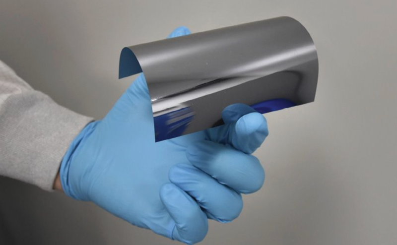
NexWafe, located in Freiburg im Breisgau, Germany, is using a unique direct gas-to-wafer method to make monocrystalline silicon wafers. The process of the manufacturer of traditional wafers is energy-intensive one, because it requires additional steps such as polysilicon refinement and ingot pulling. In contrast to this, NexWafe’s method does not require these steps, and the growth of silicon wafers can be done directly from cheap raw materials in a continuous production line.
It does not only reduce the raw material consumption drastically but also the overhead of production. None of the traditional supplemental processes is necessary, and the developers claim that with their technique the manufacturing of wafers can be done at the same time cheaper and more environmentally friendly. The company reports that its solution is capable of decreasing the cost of wafer production by up to 30% while also reducing carbon dioxide emissions by 70%, which is very beneficial for the European industry as it helps it to become less dependent on emissions-heavy supply chains that are currently dominated by Asia. At the same time, the manufacture of ultra-thin wafers is not affected in any way and the output is still compatible with the existing solar cell lines, which means that the material needs can be further reduced.
Just recently, NexWafe has managed to accomplish quite a few major technical milestones. As of December 2024, the company was able to demonstrate an efficiency of 24.4% for a heterojunction solar cell that was fabricated with its ultrathin wafers. Besides that, it revealed a 28.9% efficiency for a perovskite-silicon tandem cell, which was developed in cooperation with the Swiss Center for Electronics and Microtechnology, as a result, the technology is well-positioned for the next-generation photovoltaics high-efficiency push. According to the firm, introducing EpiWafers is the way module manufacturers can raise conversion efficiency without costly factory upgrades—an essential factor as the industry is in a race to fasten the efficiency while concurrently cutting the manufacturing carbon footprints.
With a budget of €171 million the European Commission will award these eight companies with projects in Germany, France, and the Netherlands. The other winners operate at the cutting edge in such areas as laser-driven fusion, space operations, and photonic quantum computing. It suggests that the focus of Europe is on establishing sovereignty in deep-tech sectors that are strategically important. Moreover, all eight winners, together with 21 additional applicants, have been awarded the STEP Seal, which is meant to facilitate access to alternative or complementary funding sources.
The STEP Scale Up call is an integral part of a large-scale European industrial strategy aimed at keeping the continent in pole position for strategic technologies such as clean energy, semiconductor innovation, AI, and advanced materials. The initiative got a €300 million grant and the same budget is planned for 2026 as well. There is no deadline for submission, they are accepted through the Commission’s funding and tenders portal continuously, and the evaluation rounds take place quarterly; the next selection session will be on February 11, 2026.
European policymakers, as a result of growing geopolitical tensions, vulnerabilities in the supply chain, and competition from heavily subsidized markets, have put forward the necessity of increasing domestic production capacity for solar panels. By aiming at lessening manufacturing reliance on imported components and energy-intensive production methods, NexWafe’s technology would be a good fit for these objectives.
This recent investment is a big step on the road NexWafe is taking as it moves from pilot-scale operations towards commercial production on a large scale. The money will be used to speed up the process of setting up production capacity in Europe, facilitate the development of higher-efficiency solar cells, and, in addition, contribute to the EU’s wider renewable energy goals.
Should NexWafe succeed, it will be instrumental in Europe’s solar manufacturing value chain reconstruction effort and solar panel making will become more competitive with Asia predominant producers, thereby changing the technological and economic aspects of the global photovoltaic industry landscape.